Computers Continually Follow the Fetch decode execute Cycle
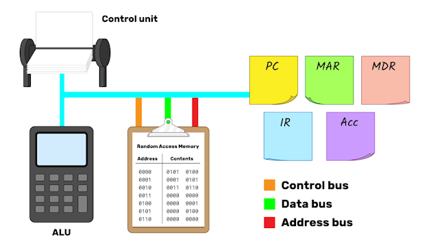
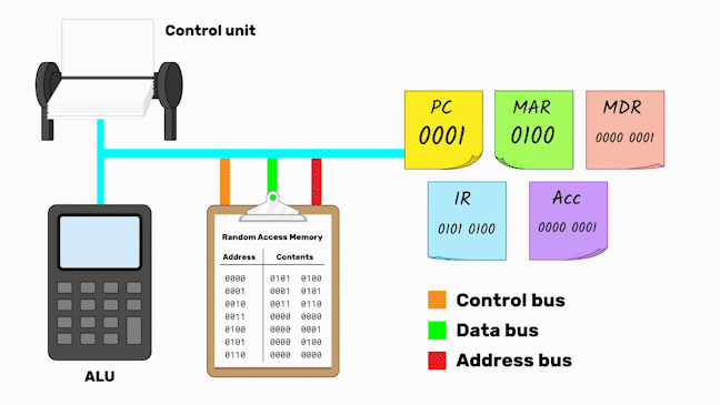
Now you are going to look at how the CPU can perform calculations, using a process known as the fetch-decode-execute cycle. Here, you have a representation of a CPU and RAM. The registers are also shown, where data can be temporarily stored.
Now you are going to look at how the CPU can perform calculations, using a process known as the fetch-decode-execute cycle.
Here, you have a representation of a CPU and RAM. The registers are also shown, where data can be temporarily stored.
Fetch
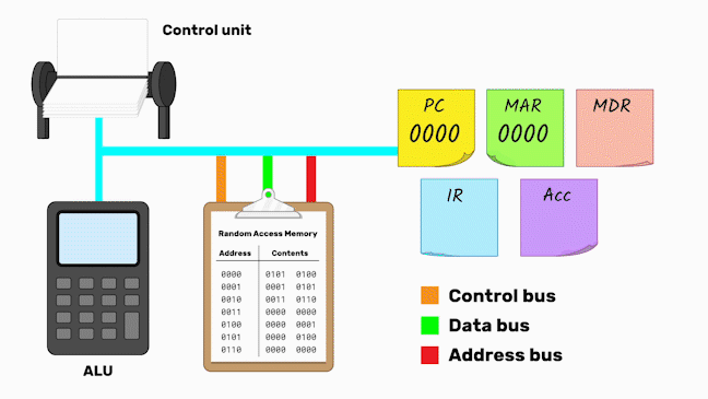
The program counter (PC) starts at 0000. This means that the first address in RAM where the computer will look for an instruction is 0000.

The computer needs somewhere to store the current address in RAM that it is looking for. This is what the memory address register (MAR) is for. The address 0000 is therefore copied into the MAR.

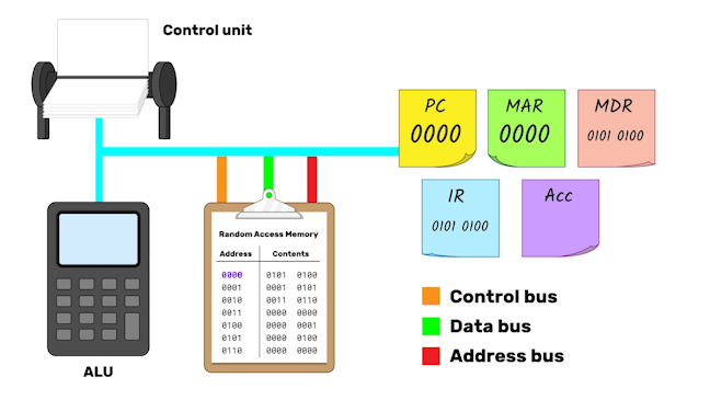
A signal is now sent down through the address bus to the RAM. The control unit sends out a memory read signal, and the contents of the address 0000 are copied through the data bus to the memory data register (MDR).
As the data fetched during the fetch stage is an instruction, it is copied into the instruction register (IR).
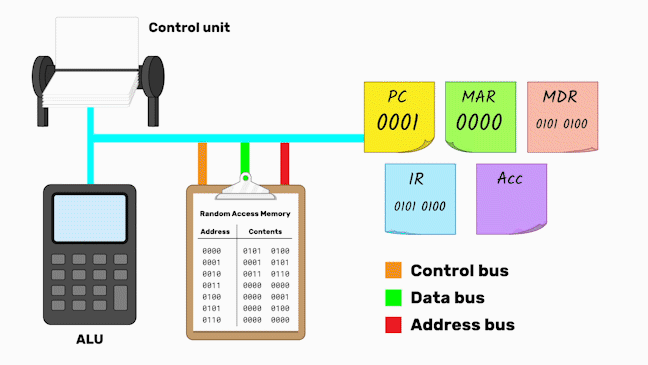
As the first instruction has been fetched, the system is at the end of the fetch stage of the cycle. The program counter can be incremented by 1, so the system is ready to read the next instruction when the next fetch cycle starts.

Decode
Now, the instruction needs to be decoded. It is sent via the data bus to the control unit, where it is split into two parts. The first part is the operation code or opcode, which in this example CPU is the first four bits. This is the command that the computer will carry out. The second part, in this case the second four bits, is the operand. This is an address in RAM where data will be read from or written to, depending on the operation.
The control unit can translate opcodes into instructions. So here the control unit translates the opcode 0101 into a LOAD FROM RAM instruction.

Execute
Now, the command will be executed. The operand is copied to the MAR, as it provides the address of the data to be loaded (0100 in this case).
The data at address 0100 is then fetched from RAM and passed up the data bus to the MDR. As it is not an instruction but simply data, it is then passed to the accumulator (Acc).
This is a complete fetch-decode-execute cycle.
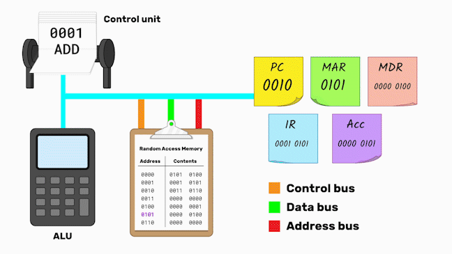
The 2nd Fetch, Decode and Execute Cycle
You will now run through the remaining two cycles of the program. The PC now holds 0001, so you fetch, decode, and execute the instruction at that address.
- The PC is at 0001, so this is the next instruction to be fetched.
- The instruction opcode and address operand are placed in the IR, and the PC increased by 1 again.
- The instruction is decoded, while the address of the data to be acted upon is placed in the MAR. The instruction turns out to be ADD, which adds two pieces of data together.
- The new data is fetched from the address and eventually ends up in the accumulator, along with the results of the previous cycle.
- To finish off this stage, the two values in the accumulator are passed into the ALU, where they can be added together, as was instructed by the opcode.
- The result is then placed back into the accumulator.
That's a second cycle complete.
The 3rd Fetch, Decode and Execute Cycle
The last cycle is for the instruction at 0010. It uses the opcode 0011, which is STORE and the operand 0110, which is the last address in the RAM shown.
So this cycle takes the results of the addition in the accumulator and stores it back into RAM at address 0110, as requested.
To recap, our program used three instructions to add two numbers and store the result in memory:
- The first instruction LOADed a piece of data from a specified address.
- The second ADDed this to the data found in another address.
- The final instruction STOREd the result of the addition back into a specified address in memory.
There is a lot of information to take in to understand the fetch-decode-execute cycle. Many people find it confusing when following it for the first time. You may find it helpful to run through this activity a second time.
Source: https://www.futurelearn.com/info/courses/how-computers-work/0/steps/49284
0 Response to "Computers Continually Follow the Fetch decode execute Cycle"
Post a Comment